Current location:Home > News >
author:admin Release time:2021-09-10 number of visits:0
The compatible fast charging mobile power supply scheme is designed and implemented by edp3010 + edp3012, which is the SOC chip of mobile power supply provided by Yineng Microelectronics Technology Co., Ltd. the general advantages of the scheme are as follows: Edp3010 chip: It is a power management SOC chip designed for PD mobile power supply. The chip application can realize complete PD mobile power function without adding additional circuits. The chip can support various interfaces such as ABC / AAC to support 36W, 45W, 65W and 100W output power (adjustable). The chip is internally integrated with pd2.0, qc2.0, qc3.0, bc1.2 DCP fast charging protocol. Pd2.0 supports 5V, 9V, 12V, 15 V, 20V full range voltage; also integrated charge and discharge management module, LED indicator module, battery balance module, battery high and low temperature protection, battery overcharge and over discharge protection, output overvoltage, undervoltage, short circuit protection, current overcurrent protection, adapter undervoltage / overvoltage protection and current self adaptation and other multiple safety protection functions; the chip supports voltage rise and fall control functions. Edp3012 chip: It is a SoC chip designed for fast charging mobile power supply; qc2.0/3.0, pe1.0, bc1.2 DCP, apple 2.4a fast charging protocol are integrated in the chip; charge and discharge management module, LED indicator module, battery overcharge, over discharge protection, high and low temperature protection, output over-voltage, under voltage, short circuit protection, current over-current protection, input over-voltage / under voltage protection and current adaptive function are also integrated Heavy security protection function; the chip supports double port random insertion and quick release function (any a port can be inserted to realize quick release, and then when another mobile phone is inserted, it will drop to 5V and discharge at the same time); support side charging and side releasing: first charge the mobile phone, then charge the battery after the mobile phone is full. Support AABC interface form. After sales guarantee: Huaqiang core city provides product quality service, and China Electronics Technology Co., Ltd. * * * * agent provides technical support. Scheme reliability: high reliability, the scheme is provided by the authorization of YENENG Microelectronics Technology Co., Ltd., the scheme has undergone five times of optimization and modification and finally formed; the main chip of the scheme is also provided by the authorization of YENENG, the reconfigurable power supply IC of YENENG has complete independent intellectual property rights, at present, it has obtained 11 intellectual property rights, 7 utility model patents, 2 integrated circuit layout design; One invention patent, one computer software copyright acceptance, won the 2014 EET * * power chip award, 2015 EET, EDN, ESM * * Power Management IC award, 2015 "China core" * * * * potential product award of Ministry of industry and information technology, the company also won the honorary title of the 4th China science and technology innovation and entrepreneurship competition information industry.
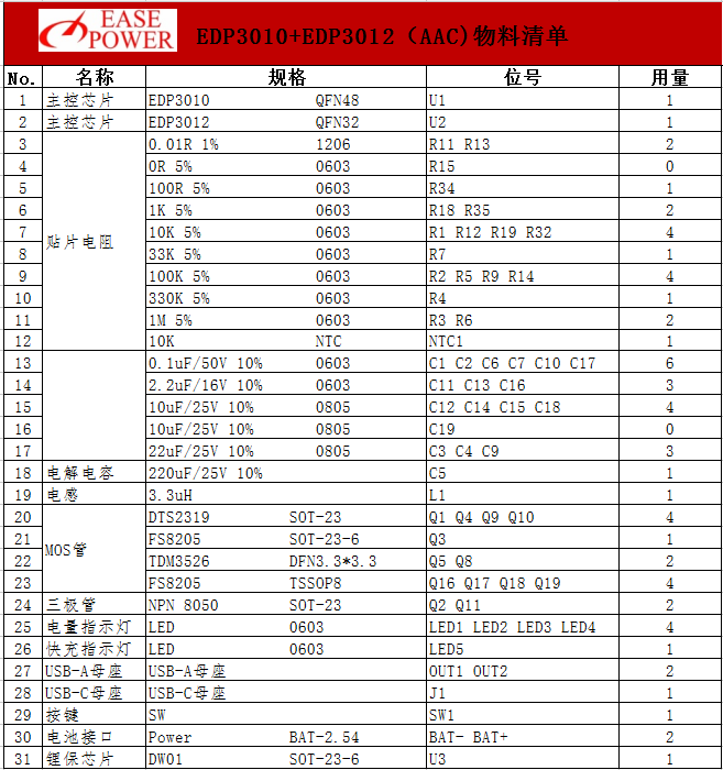
BOM BOM:
EDP3010
◆ 多串 PD 快充移动电源
◆ 车充
◆ 适配器
EDP3012
◆ 快充移动电源
◆ 快充车充
◆ 智能排插
EDP3010+EDP3012: 全兼容 QC/PE/AFC/FCP/SCP/VOOC 快充移动电源方案
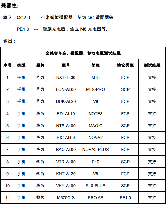
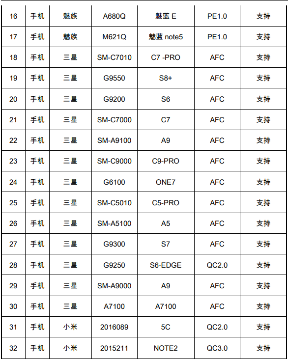
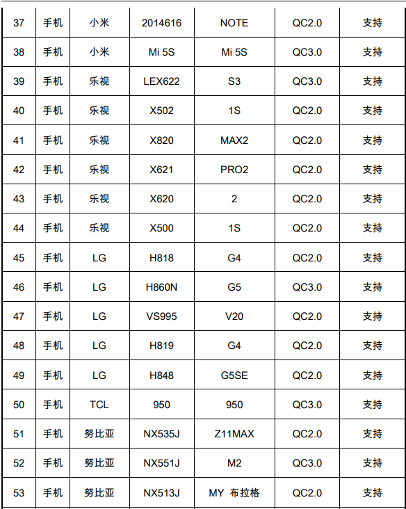
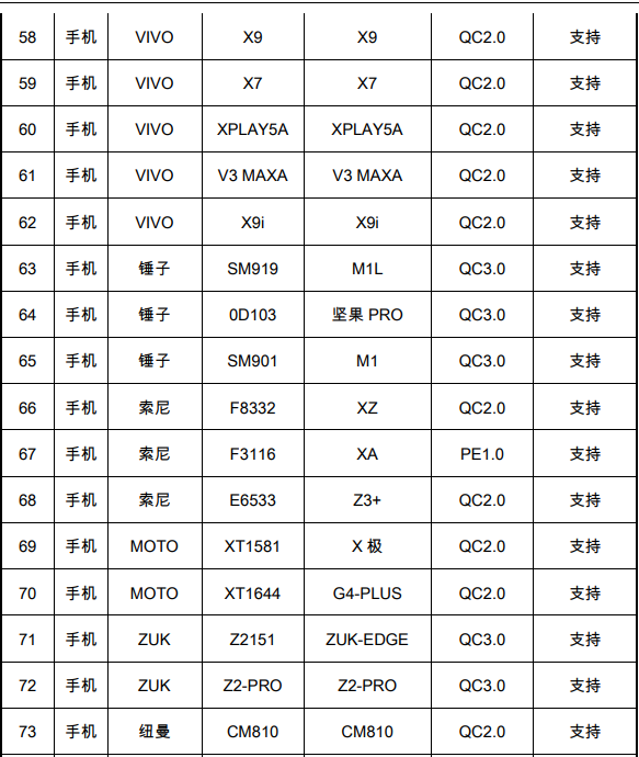
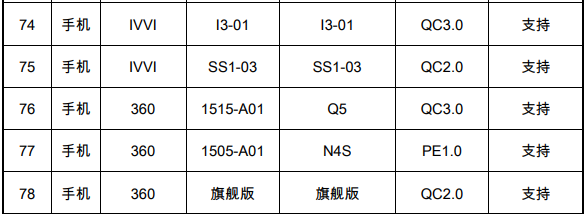
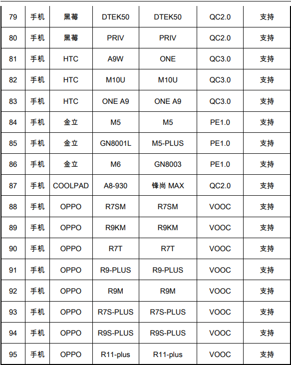
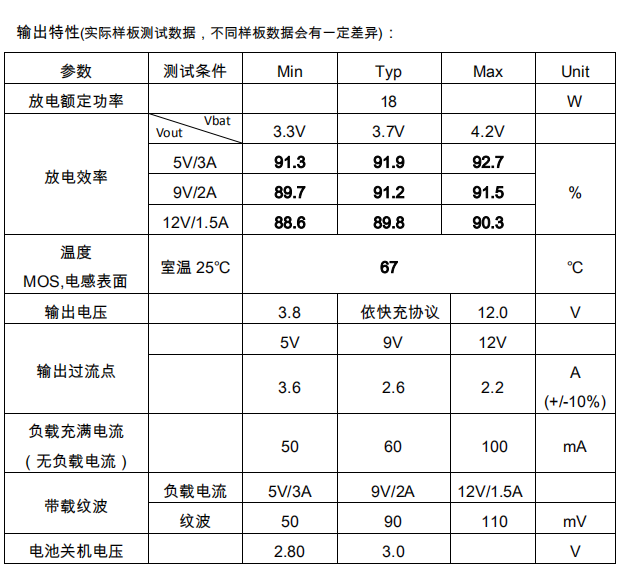
用一颗芯 片完成了 DC-DC 升降压和快充协议,方案集成度高,外围原件少,热效率非常****,18W 时 ****效率超过 90%. 元件温度低于 70℃。支持 BC1.2 DCP, QC2.0/3.0, PE1.0, AFC, FCP, SCP, VOOC, Apple 2.4A 输入输出双向快充协议. 测试了市场上 100 多款几乎囊括了所有快 充协议的手机,兼容性几乎做到 100%. 具有完善的电池充放电管理,独立的锂电保护电路, 支持过压/欠压,过流,反向电流,短路,高低温保护等功能. 安全性高,可靠性好,生产简单, 是当前市场上快充协议*全,兼容性****的快充移动电源方案.
✔支 持 BC1.2 DCP, QC2.0, QC3.0, PE1.0, AFC, FCP, SCP, VOOC, APPLE 2 .4A 快充协议, 兼容市面上几 乎所有快充手机
✔AAC 接口
✔额定输入输出功率 18W
✔18W ****充放电效率高于 90%
✔C 口单向只做输入
✔支持插入检测,插入自动输出;
✔两个及以上输出口都插入手机后会退出快充, 输出电压降到 5V;
✔输入电流自适应 输出电压自适应
✔NTC 检测
✔电量等级 4 个 LED 指示, 独立的快充 指示 LED
✔电芯电压 4.20V, 4.30V,4.35V,4.40V 可 配置
✔4 个等级电量电压点可配置
✔过流, 反向电流,过压/欠压,短路,高 低温保护
Q&A
Q1:电池的电压不同,如何配置?
A2:可以提供4.20V,4.30V,4.35V,4.40V四种电芯电压的软件
Q2:每款电池的放电曲线不同,如何配置?
A2:方案中用4个LED灯来表示电池电量等级,可以根据客户电池的放电曲线通过软件调整电量等级的电压值;
Q3:输入输出接口外壳是否可以接GND.
A3:不可以.因为某些接口连接线负极是与外壳相连的,而我们的采样电阻要接在GND与接口负极中间若两者相连则相当于采样电阻 短路了。

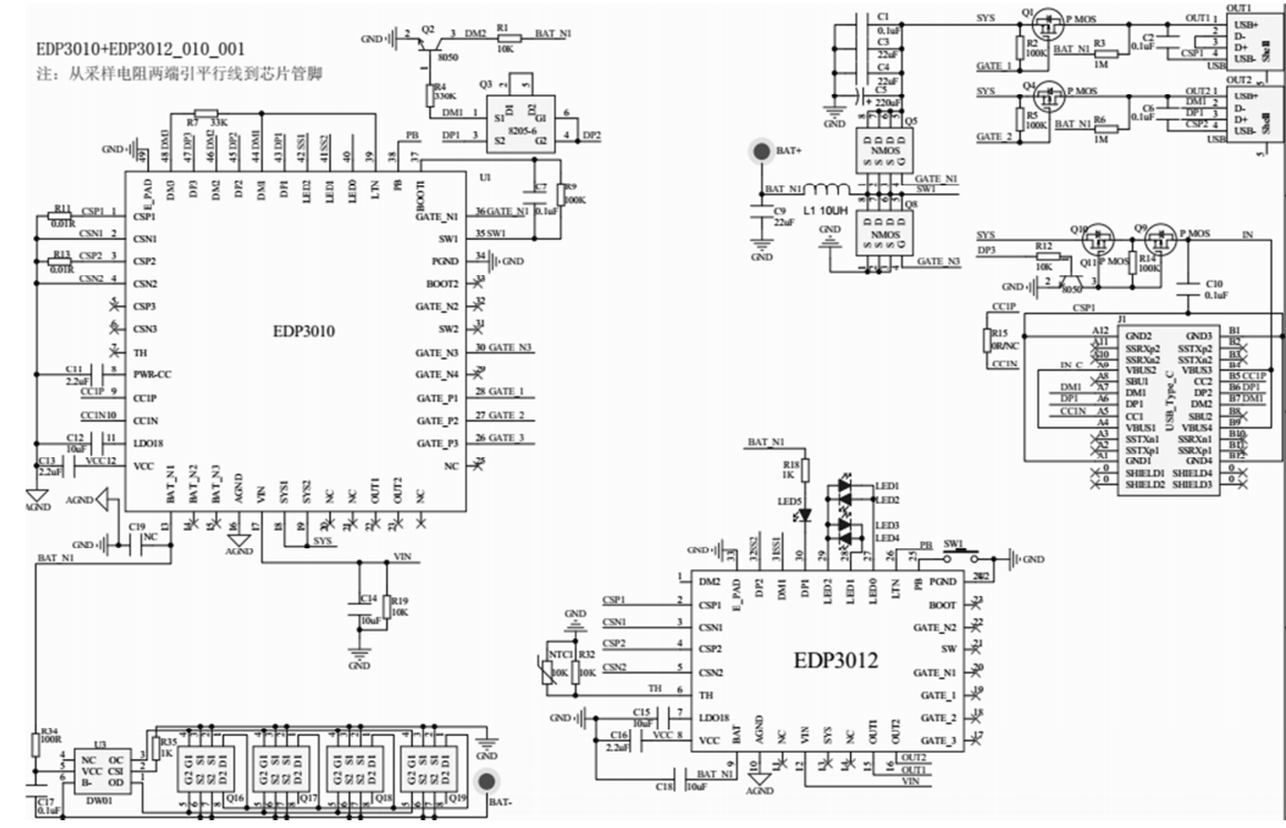
电路图:
PCB设计参考:
1.IC下面需敷铜散热(IC 衬底要连接到 PGND),散热面积尽量大,衬底焊盘打通孔到PCB底层,并适当露铜皮增强散热。
2.LDO18脚的10uF电容要靠近芯片管脚;AGND用单点接连的方式回到PGND。
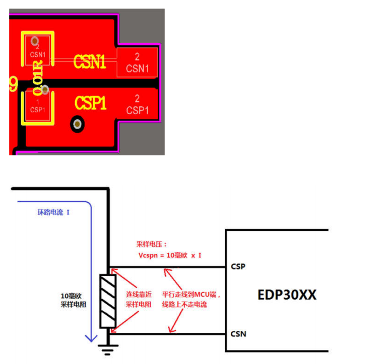
3.采样电阻CSP,CSN端Layout应遵循如下规则:
a) CSP,CSN走线要尽量避开干扰源器件比如电感,环路MOS,Vout等;
b) CSP,CSN走线尽量在同一层,减少打孔的情况;
c) CSP,CSN两条线都尽量靠近芯片;采样电阻到芯片端之间的连线不得过电流.同样原理CSN也是不可以直接和PGND相连。
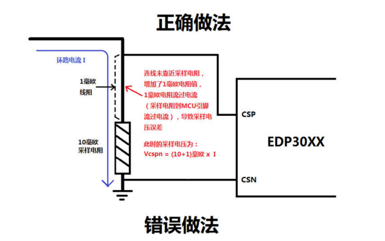
4.大电流通路(升降压环路部分电路:BAT–电感–MOS-VOUT):尽量走在同一层,而且尽量粗短,同时地的面积也尽量增大且要完整.这样可以增加散热,减小EMC干扰.
5.USB口外壳不可以直接接 GND. 因为某些USB线负极是与外壳相连的,而采样电阻是需要接在接口负极与GND中间,若两者相连则相当采样电阻短路了.
6.为保证散热,EMC等性能****,推荐使用四层板.
| 标准板规格书: | EDP3010+3012 全兼容QC,PE,AFC,FCP,SCP,VOOC快充移动电源方案_v1.31_20171226.pdf |
| IC规格书: | 3010+3012.pdf |
| BOM List: | EDP3010+EDP3012_010_001(AAC).xls |
| 参考LAYOUT Gerber: | PCB设计注意事项_v1.00_20171225.pdf |
| 电路图: | EDP3010+EDP3012_010_002(AAC).pdf |
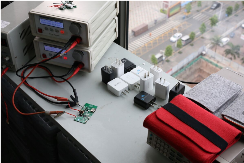
一、输出功率、效率、温度、兼容性测试
测试环境如下:
兼容性测试:
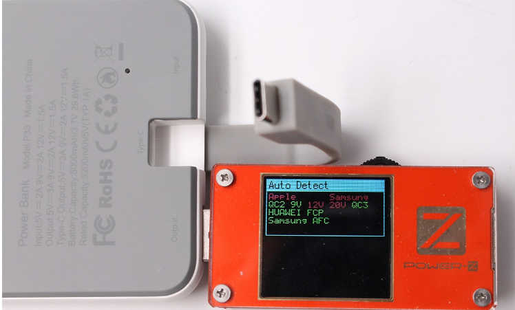
表头显示支持QC2.0、QC3.0、FCP以及AFC快充协议。
开机熄屏、关机状态下,易能微EDP兼容性:
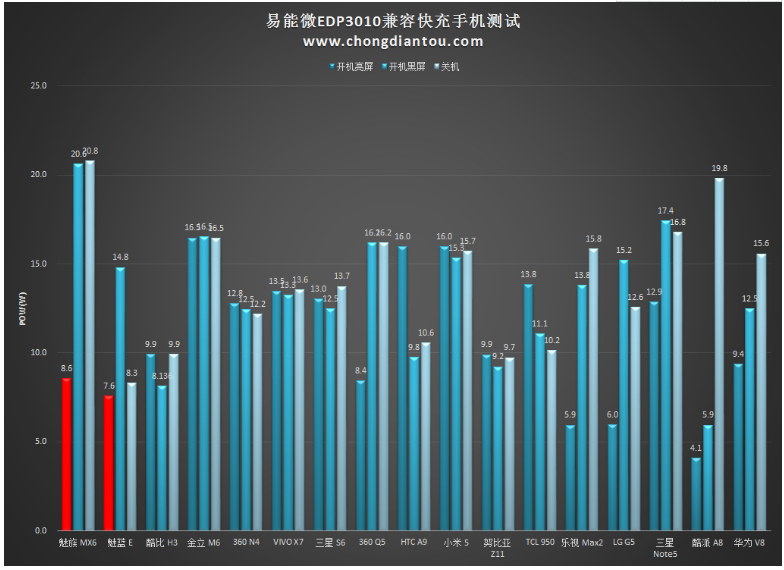
不同输出电压平台转化效率:

温度测试:
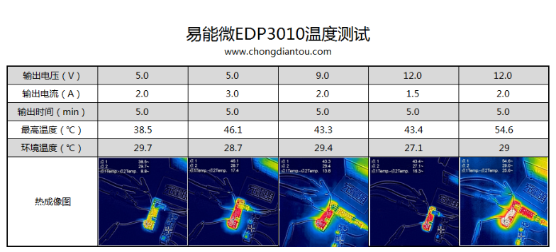
二、横向对比:
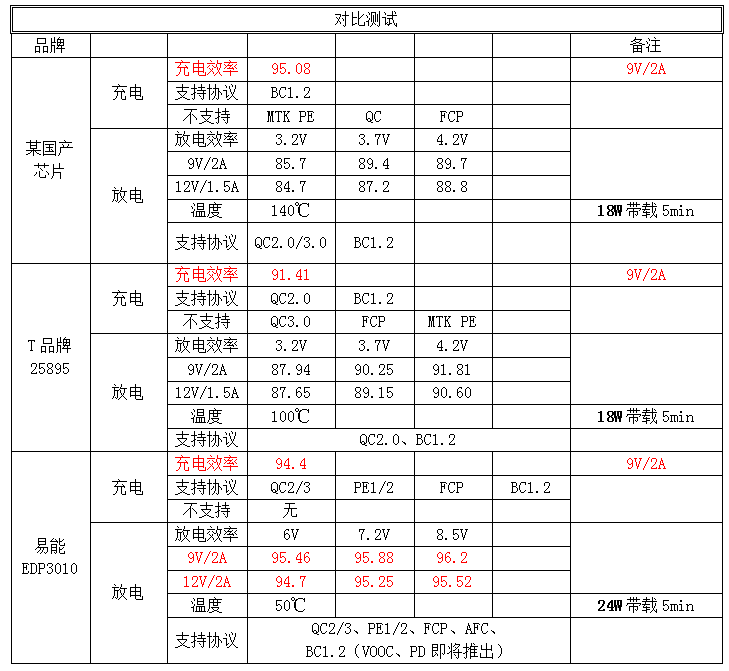
三、18W全兼容快充移动电源方案兼容性
